
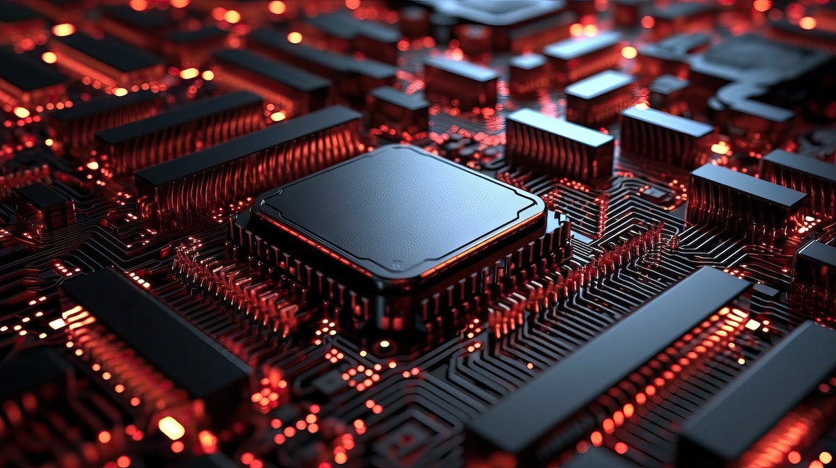
The semiconductor industry depends on precision and efficiency to meet the increasing demand for smaller, faster, and more powerful devices. As these devices shrink in size, the need for advanced tools to analyze materials at the atomic level becomes increasingly important. Erik Hosler, an expert in light source development, notes that advanced light sources like free-electron lasers (FELs) are transforming the way manufacturers approach material analysis. These advanced technologies offer the precision needed to refine semiconductor fabrication processes and produce higher-quality devices.
The Role of FELs in Material Analysis
Free-electron lasers generate highly focused, tunable beams of light that allow manufacturers to examine semiconductor materials in unprecedented detail. By adjusting the wavelength of the laser, FELs enable a thorough inspection of both the structural and chemical properties of materials, providing insights that are critical for the development of next-generation chips. This analysis is crucial for detecting even the smallest defects in semiconductor materials, which can compromise device performance.
With the ability to probe deep into the atomic structure of materials, FELs allow manufacturers to optimize their processes and reduce the likelihood of defects, leading to higher production yields and more reliable chips. This capability is particularly important as the semiconductor industry continues to push the boundaries of miniaturization, where even the slightest material imperfection can result in a significant loss of efficiency.
Enhancing Precision in Semiconductor Fabrication
In addition to improving the quality of materials, FELs contribute to overall precision in semiconductor fabrication. These light sources provide detailed information that helps manufacturers fine-tune their processes, from material selection to component integration. This level of precision gives manufacturers greater control over the production process, ensuring that each stage of fabrication meets modern chip manufacturing’s strict standards.
Erik Hosler, who has been at the forefront of these developments, explains, “Accelerator technologies, particularly in ion implantation, are enabling manufacturers to push the limits of miniaturization while maintaining the integrity of semiconductor devices.”
As the demand for more powerful and energy-efficient chips continues to rise, advanced light sources like FELs will play an increasingly important role in semiconductor fabrication. These tools offer the precision and efficiency needed to meet the challenges of future chip designs, helping manufacturers maintain their competitive edge. By revolutionizing material analysis, FELs are paving the way for the next generation of semiconductor technologies.